DIY Curve Tracer
Posted by Thomas A. Kilbride, , 0 comments.

  • Abstract
  • The purpose of this experiment was to build a curve tracer to measure the characteristics of a Bi-polar Junction Transistor (BJT). The experiment found that it is possible to use a curve tracer to measure the forward DC amplification factor β of a BJT. It was concluded that a curve tracer is useful for quickly characterising BJT's. Additionally, these measurements can be used to find matched pairs of BJTs (i.e., two BJTs with a similar β measurement).

    Introduction

    BJTs are often used in analog circuits where current amplification is needed. The equation which models the current gain of a transistor is given by: \begin{equation} \label{eq:1} \beta I_B = I_C \Longleftrightarrow \frac{I_C}{I_B}=\beta \end{equation} In the equation above, the current gain of the transistor (β) is defined by the ratio between the BJT collector and base currents. Unfortuinately, not all transistors have the same β due to deviations in manufacturing. The deviations in β need to be considered when constructing circuits such as a differential amplifier. If the amplification factors are too dissimilar, a circuit will not behave as expected. In order to measure these parameters, a family of curves for each BJT needs to be obtained. To obtain a family of curves for a BJT, one must perform a Collector-Emitter voltage DC sweep at targeted base-current operating points. A curve tracer streamlines this process by sequentially constraining a different $I_B$ before performing a DC sweep for each setting.

  • Theory
  • A 4-bit Binary Counter (74HC193)

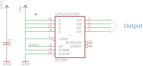
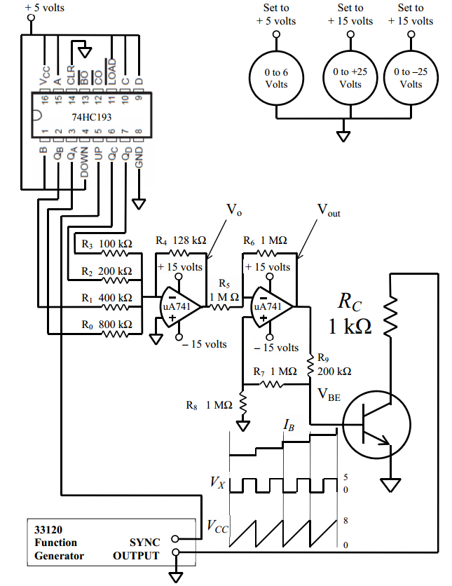
    The binary counter is the first stage of this circuit. This stage utilizes a 74HC193 integrated circuit and can be realized by sequentially cascading four D-latches:.
    The SYNC output of the function generator is used as the clocking signal in the diagram above and it is also in phase with the collector-emitter DC sweep. When the sync pulse is pulled high a new collector-emitter DC sweep starts and the binary counter also increments. The following is the timing diagram for the outputs of the 74HC193, where the clocking signal is the SYNC pulse from the function generator:

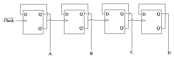
    N-Bit Digital-to-Analog Converter (DAC)

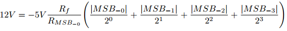
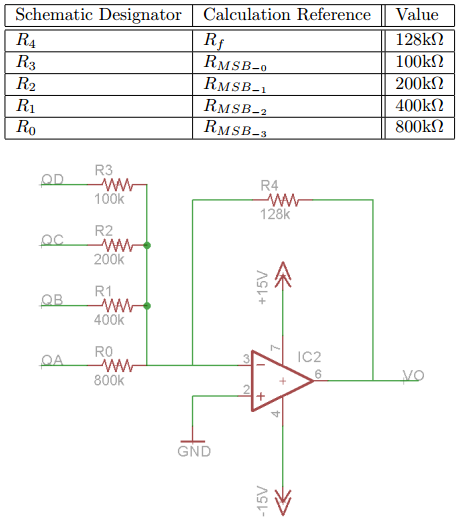
    The second stage of the circuit will convert the binary counter's output registers to an analog waveform by adding them while accounting for the significance of each bit. An operational amplifier in a summing configuration is used to achieve this task:
    Note: because the SYNC input pulse to the binary counter is in phase with the collector-emitter DC sweep sweep, it will create a zero-order hold at the output of the summing amplifier. The hold time is equivilant to the phase of the collector-emitter DC sweep sweep. The output from DAC will look like a decreasing sawtooth wave with some aliasing and inversion because the op amp is in an inverting configuration:
    By referencing the circuit above, the equation which models the summing amplifier configuration is given by the following KCL equations: \begin{equation} I_F = I_1 + I_2 +\dots+ I_n \\ -V_{out}=\frac{R_F}{R_{1}}V_1+\frac{R_F}{R_{2}}V_2+\dots+\frac{R_F}{R_{n}}V_n \end{equation}

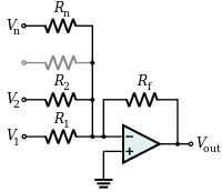
    Transconductance Inversion Amplifier

    By this stage there we have a decreasing sawtooth wave. This step will invert the waveform to get the desired increasing sawtooth waveform. An inverting amplifier with is used as a buffer in this step:
    Additionally, it is not desired to bias the BJT; therefore, this amplifier must also convert voltage to current. It must also have a very high output impedance.

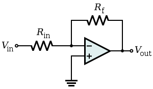
    Device Under Test (DUT)

    After the waveform has been inverted, it is then fed into the DUT. In this case, the DUT is a BJT. By this point each binary number is summed, the waveform is stepped up by an increment and then inverted to get an increasing aliased sawtooth wave. The output from the subsequent steps provide the base current to the BJT so the family of curves can be produced when a collector-emitter DC sweep is executed.
    In theory, these two sweeps should produce a family of curves when measured on an oscilloscope.

    Measurement

    An oscilloscope and differential amplifier are used to obtain the family of curves using the XY plotting feature of the scope's display. The reason a differential amplifier is used is so the probe's impedance does not divide current from small voltage measurements.

  • Design
  • Up Counter

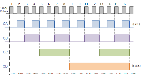
    As discussed previously, the binary counter is connected to the sync pulse. In this application it is correct to call it an Up-Counter; in theconfiguration used the DOWN pin is pulled high while the UP pin is pulsed. When the up counter reaches its terminal value it rotates back to the base. The following timing chart shows the outputs of the 74HC193 as it counts from 0 to 10 in the up-coutner configuration:
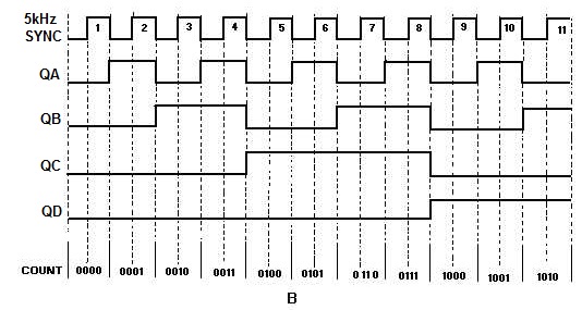
    The circuit implementation for the up counter stage used in the experiment is the following:
    The power supply rail has a bypass capacitor inserted located as physically close to the IC as possible. This capacitor helps decrease the noise on the outputs as they change between binary states. The precise value of a bypass capacitor isn't important but generally speaking a higher capacitence means it can provide more damping of supply ripple voltage. A common value of 0.1$\mu$F was used in this design (reference C1 in the schematic above).

    4-Bit DAC

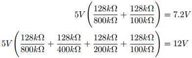
    Since we are adding 4 bits from the counter, this stage of the design needs four inputs. These inputs create the linear terms necessary in the KCL equations. The input resistances (R1, R2, R3, R4) are calculated so the output of the amplifier accurately reflects the magnitude of the counter for each cycle. This table shows the magnitude weighting of each binary value relative to the other:
    These relative weights tell us that the input resistances must satisfy the following equation: \begin{equation} R_{MSB_{-0}} = \frac{1}{2}R_{MSB_{-1}}= \frac{1}{4}R_{MSB_{-2}}= \frac{1}{8}R_{MSB_{-3}} \end{equation} Another constraint in the design is the DAC's full-scale output voltage. It must be adequately high so that in the following stages it can set $I_B$ at a reasonable point. Additionally, it cannot be so high that it goes beyond the supply rails for all following stages (causing clipping in the next step or in the DUT).The full-scale voltage of the DAC is targeted to 12V. This means that with an input of 16 the DAC's output will be 12V. Constraining the full-scale equations gives the KCL following equations: \begin{equation} 12 V= -5V \frac{R_f}{R_{MSB_{-0}}}\Bigg( \frac{|MSB_{-0}|}{2^0} + \frac{|MSB_{-1}|}{2^1} + \frac{|MSB_{-2}|}{2^2} +\\ \frac{|MSB_{-3}|}{2^3}\Bigg) \end{equation} Solving for one of the resistor weights gives:
    Using (6) to calculate the other input resistances gives the complete set for the DAC with the schematic:
    The following are two sample calculations given the states of 10 and 16:
    (10) implies that two cycles of the output at this stage should look like the following graph when the the up counter changes its output registers:
    As expected, the output of the 4-bit DAC is decreasing due to the fact that it is in an inverting configuration.

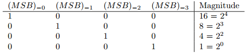
    Transconductance Amplifier

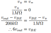
    As discussed in the theory section, the inverting amplifier's output is given by \eqref{3}. Additionally, the amplifier is in a unity gain configuration, this means that the input resistance to the amplifier is equal to the feedback resistance. Therefore: \begin{equation} V_i=-V_o \end{equation} Furthermore, we want do not want the output to offset the DC base-emitter voltage; therefore, the output resistances make this function as a transconductance amplifier. The circuit realization of this component is the following:
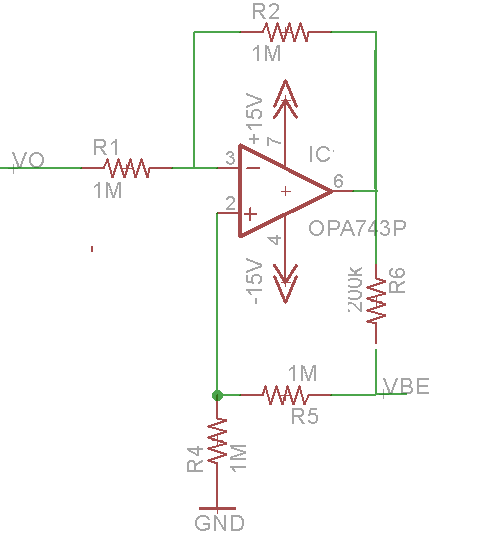
    The following are the calculations relating the input voltage from the DAC (VO) to the output voltage to the DUT (VBE). The op-amp is modeled as ideal:
    Next we must write the output current as the current delivered to the base: \begin{equation} I = I_1 + I_2 + I_B \end{equation} \begin{equation} I_B = \frac{v_{out}-v_{BE}}{200k\Omega} - \frac{v_{BE}}{2M\Omega} \end{equation} By combining the equations: \begin{equation} I_B = -\frac{5v_{out}}{200k\Omega} \end{equation}

  • Results
  • Circuit Diagram

    Plots

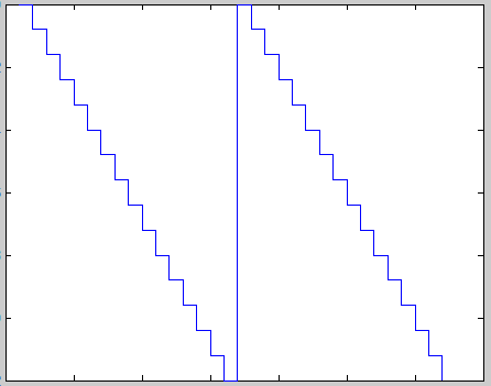
    For some reason I cannot find the plots for this project; however, the hardware did work as intended. The only problems I found were some resoluution issues which could be solved by using a better DAC, one with a 16-Bit resolution could improve this performance.